Scanning Tunneling Microscope experiments
Electronics, Projects ·Introduction
It was in a physics lecture at HTL when the teacher told us about a microscope capable of depicting individual atoms. The principle fascinated me, so I started to read about it. Usually, such instruments are hugely expensive and, with all accessories, can fill an entire room. But to my great surprise, there are actually hobbyists who build such a device with relatively simple means and tools. Not all of those projects achieve atomic resolution, but still it would be an extremely fascinating project.
The experimental setup
I started to build a prototype hardware, which is inspired by many different hobby projects that could be found on the internet. The design is based on the genius piezo scanner invented by John D. Alexander, which is made from a simple piezo speaker. The scanner is capable of moving a tungsten needle in all three space directions. The range, however, is very small, only a few micrometers. To bring needle and measurement sample in the region of the piezo scanner, a coarse approach mechanism with a lever design is used. The parts are manufactured from granite, with the intent to reduce thermal drift.
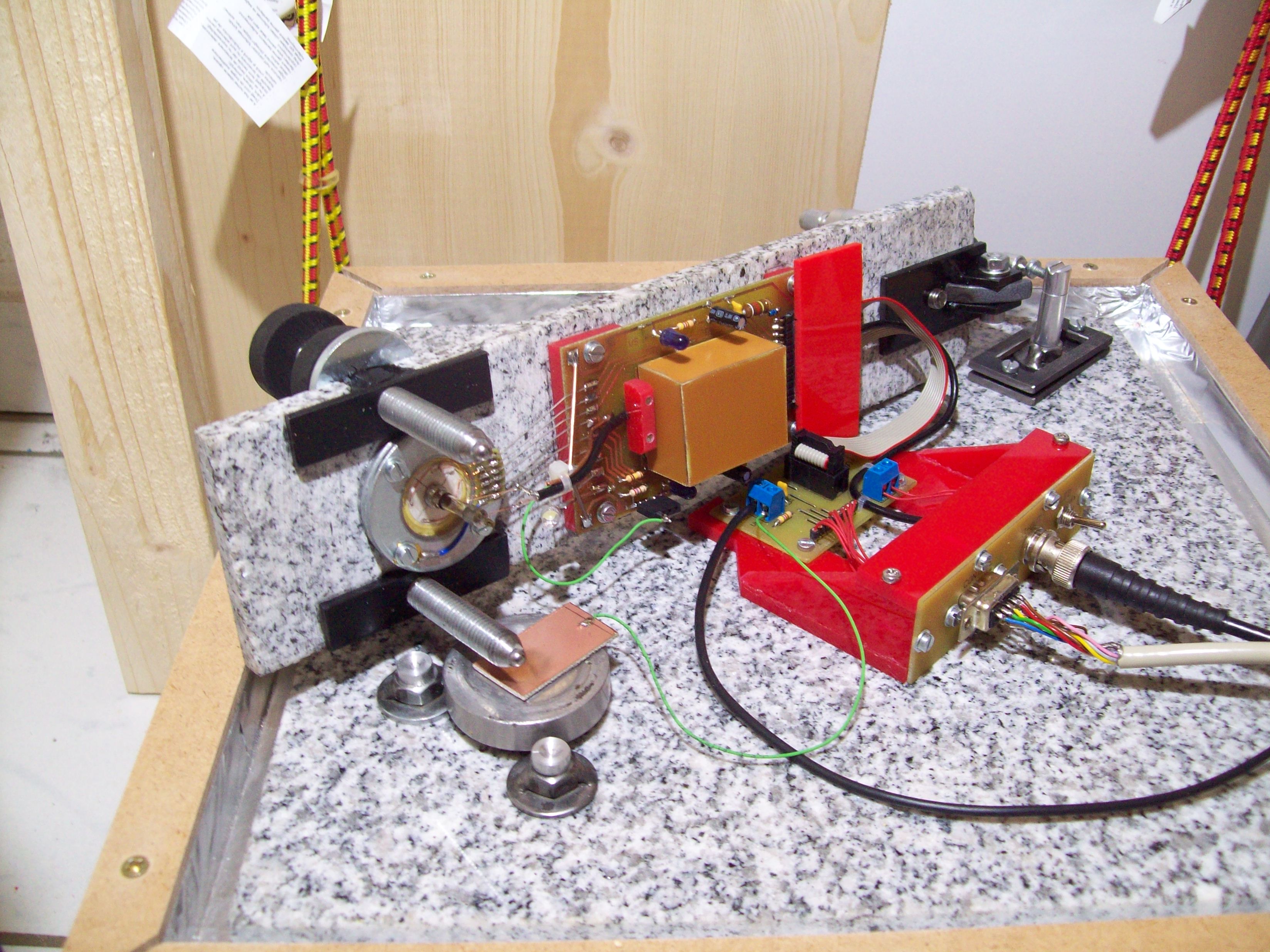
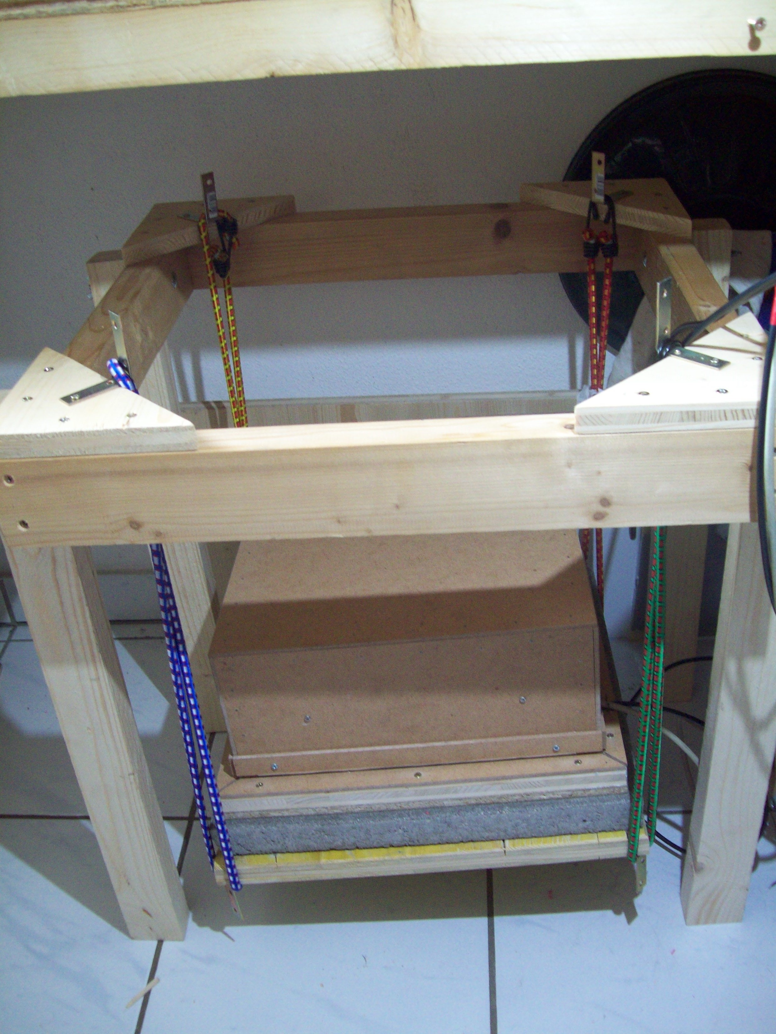
When the needle is scanned over a sample surface, a very small tunnel current starts to flow if the distance is sufficiently close. This tunnel current in the picoampere range is amplified and used as an input to a control loop that adjusts the z-height of the needle to keep the current constant. From the output signal of the control loop, the depth information is retrieved. Because distances are very small, the setup is very sensitive to vibrations. For this reason, the scanning head rests on a concrete slab, which is suspended in the air with rubber bands.
Progress so far
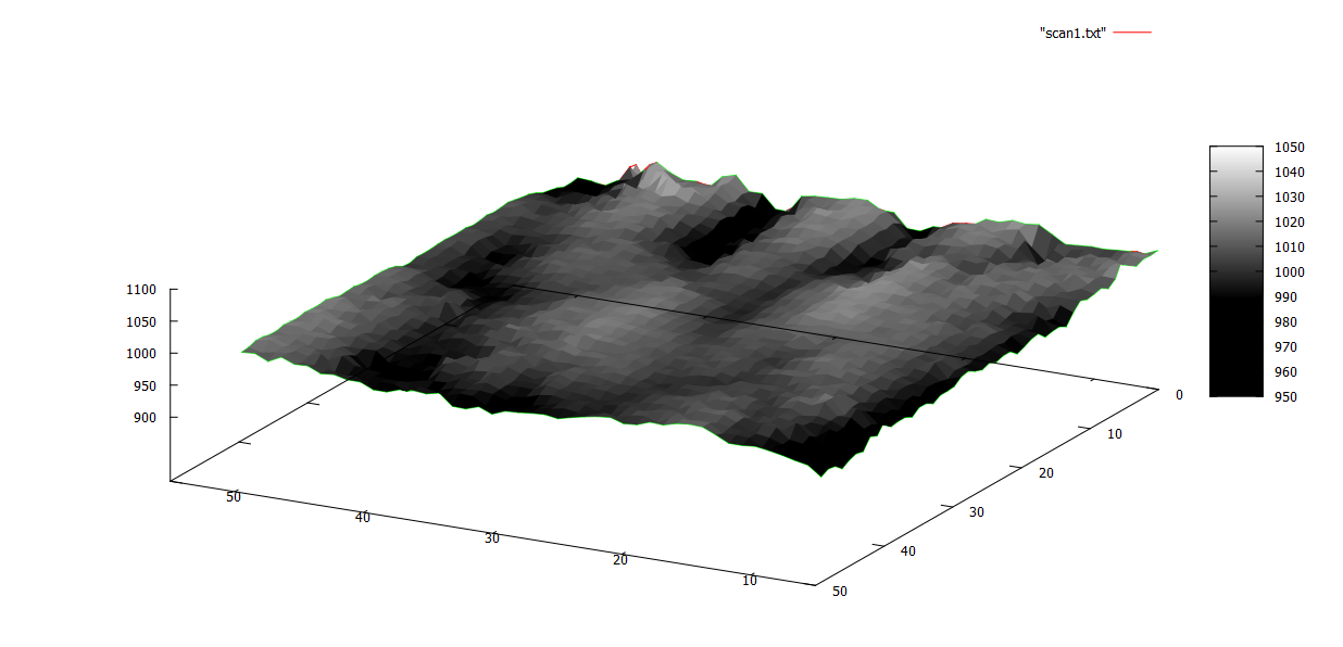
A first test scan of a copper surface with the control electronics mostly on a breadboard was carried out. The test worked in principle, as the control loop was able to keep the tunneling current constant and the individual “scan lines” formed a connected 3D-surface. There is, however, no real way for me to check how well the scan result represented the real surface.
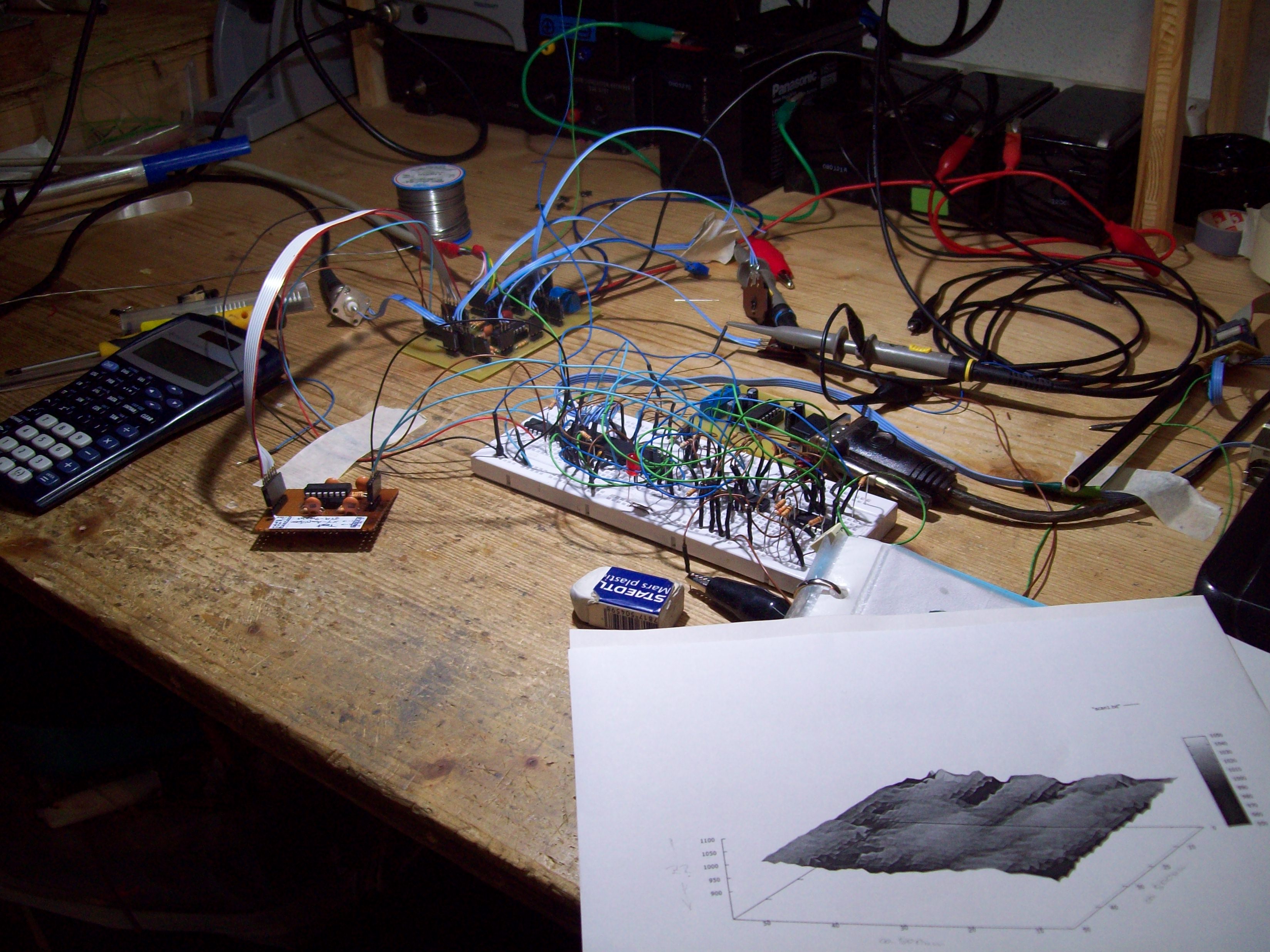
I subsequently started to lay out all the control electronics on a number of PCBs, all realized purely analog, with opamps and so on. While doing so, some doubts started to arise. All these small signals are very sensitive to noise, and the all-analog approach over different PCBs just did not seem ideal to me. I think, a much better solution would be to only realize the preamlifier and the piezo-drivers in a discrete manner, and move all the rest into a microcontroller. That way, the control parameters can easily tuned and I think the overall performance would just be much better than multiple tens of opamps.
And this is unfortunately the point where work has stopped and was not continued since. Maybe at some point if I find time for it, with more knowledge about control loops and data processing on microcontrollers, I will continue to build the electronics. At some point, also the hardware will have to be reworked because I think it can be done much smaller, which would remove lots of hassle, from the space and handling in general to thermal drift and vibration issues.